| « 2022-05-12 | Tinkering | 2021-11-06 » |
Tinkering: 2022-03-19: Alarm Clock (2)
Part 1: prototype clock, beech wood.
Part 2: this article.
Part 3: last incarnation, amaranth wood.
Part 4: alarm clock repair.
In part 1 of the Word Alarm Clock series, the prototype was presented. After the prototype was finished, the workshop was extended with more and better tools: table saw, vacuum pump, air compressor, disk sander, face shield...
And now, the second alarm clock is finished, and this part has a few more pictures and explanations.
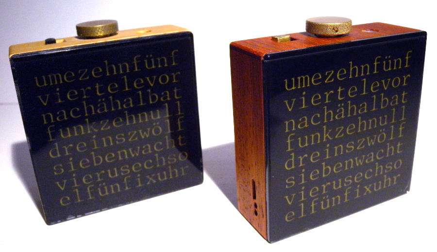 The two clocks are basically the same design on the outside, but a few
things were changed compared to the prototype. It was clear from the beginning
that the type of wood would be different. The prototype has a beech wood
enclosure, while No.2 is made from padouk, a very beautiful red coloured
wood. It will probably become brown over time, but the grain structure is
stunning on its own.
The two clocks are basically the same design on the outside, but a few
things were changed compared to the prototype. It was clear from the beginning
that the type of wood would be different. The prototype has a beech wood
enclosure, while No.2 is made from padouk, a very beautiful red coloured
wood. It will probably become brown over time, but the grain structure is
stunning on its own.
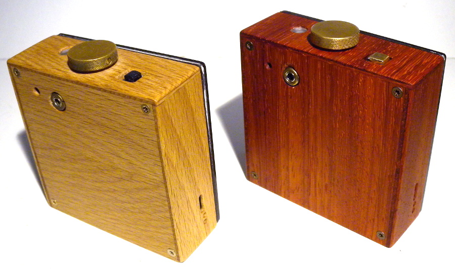 When building the new enclosure, I paid much more attention to the grain direction,
so that top, back, and bottom pieces are from one contiguous piece of wood so
that the grain is almost contiguous, too.
When building the new enclosure, I paid much more attention to the grain direction,
so that top, back, and bottom pieces are from one contiguous piece of wood so
that the grain is almost contiguous, too.
The wood I used is home-made plywood, and cutting the plies was the reason to first build the table saw (which I wanted to do anyway). The saw now cuts much more consistently than what I could do for the first enclosure's beech plywood.
The wood is finished using hard-wax oil, which makes the padouk colours darker, but also more vibrant. The camera does not fully capture the impression.
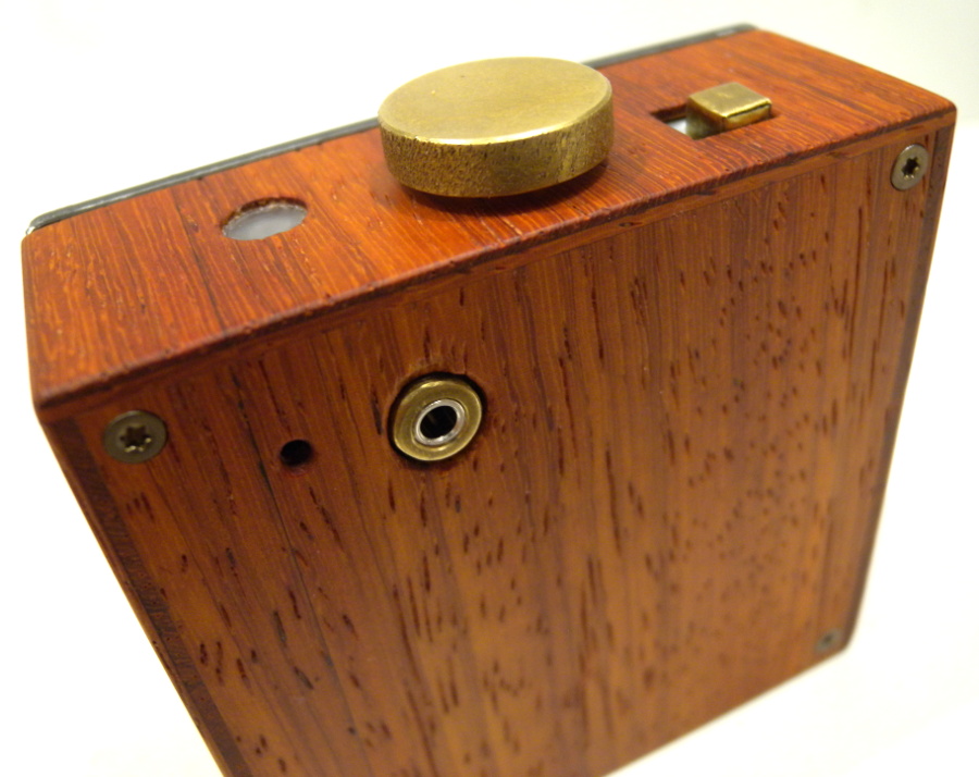 The coffee machine connector nut is now polished more nicely, and it has no slot.
The nut can only be tightened when the clock is disassembled, but that's OK,
because assembly and disassembly was also improved.
The coffee machine connector nut is now polished more nicely, and it has no slot.
The nut can only be tightened when the clock is disassembled, but that's OK,
because assembly and disassembly was also improved.
 The display was glued like before with epoxy resin, from a PCB with the face grid
and the crystal made from glass. This time, the epoxy was vented using my new
vacuum chamber, and the resin was cured in the pressure pot at 3.5 bar, which
eliminates all visible bubbles. The new clock face is much clearer
this way.
The display was glued like before with epoxy resin, from a PCB with the face grid
and the crystal made from glass. This time, the epoxy was vented using my new
vacuum chamber, and the resin was cured in the pressure pot at 3.5 bar, which
eliminates all visible bubbles. The new clock face is much clearer
this way.
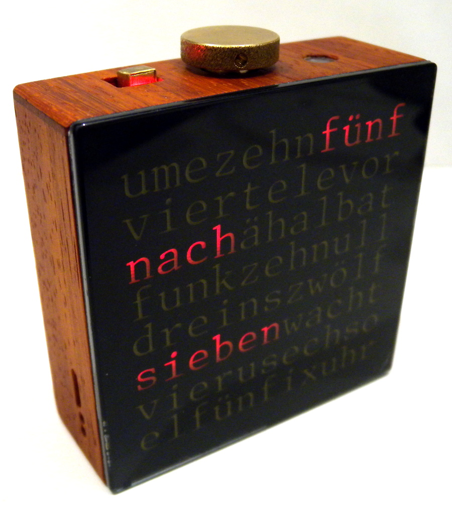
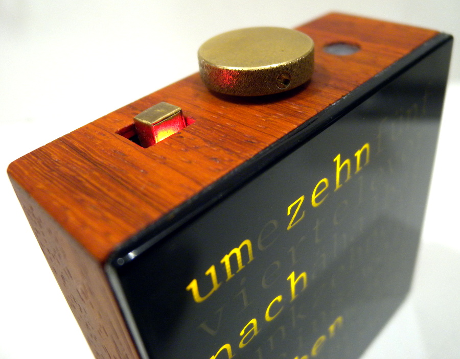 The alarm on/off switch now has a brass cap to make it a little nicer.
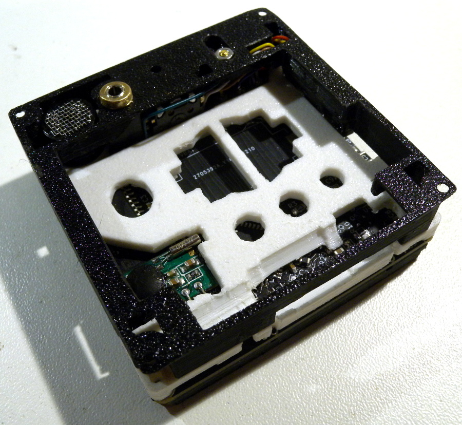
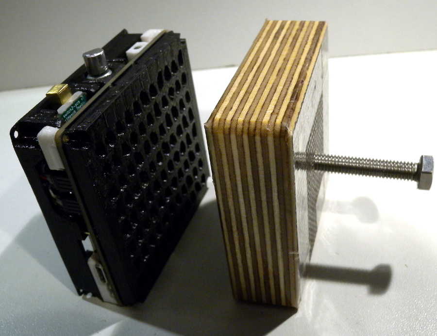
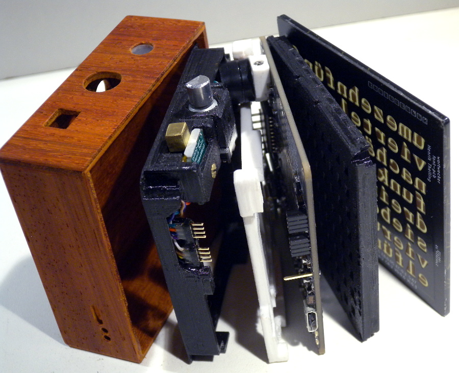 This is the sandwich structure of the alarm clock, consisting of (from left to right),
the enclosure, the switch module, the mounting frame, the control module (the main PCB),
the display spacer,
and the face and crystal. All parts are now separate and can be assembled and
disassembled more easily than in the prototype, and instead of cables, small pin
headers are used to connect the switch module with the control module.
This is the sandwich structure of the alarm clock, consisting of (from left to right),
the enclosure, the switch module, the mounting frame, the control module (the main PCB),
the display spacer,
and the face and crystal. All parts are now separate and can be assembled and
disassembled more easily than in the prototype, and instead of cables, small pin
headers are used to connect the switch module with the control module.
 To make it easier to precisely drill the holes into the enclosure, I made
a 3D printed template to guide the drills.
To make it easier to precisely drill the holes into the enclosure, I made
a 3D printed template to guide the drills.
 The enclosure is placed inside the template, can then be clamped, and then the
drill for all the holes is tightly guided. This made placing the holes quite
easy. The template can also be used as a guide for a first approximation
of cutting the enclosure to length (or, maybe height).
The enclosure is placed inside the template, can then be clamped, and then the
drill for all the holes is tightly guided. This made placing the holes quite
easy. The template can also be used as a guide for a first approximation
of cutting the enclosure to length (or, maybe height).
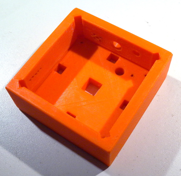
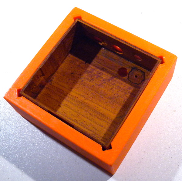
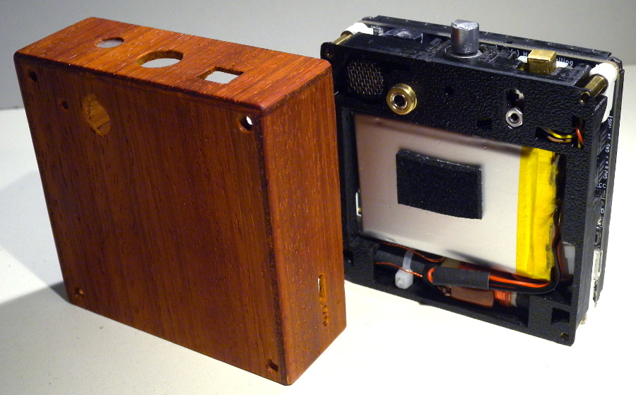
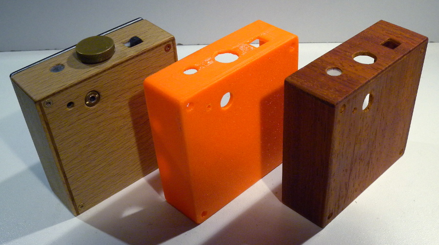 I also made a 3D printed enclosure, because it is always good to quickly have
an enclosure – building one from wood takes a while, and the inner parts may
need to be fitted.
I also made a 3D printed enclosure, because it is always good to quickly have
an enclosure – building one from wood takes a while, and the inner parts may
need to be fitted.
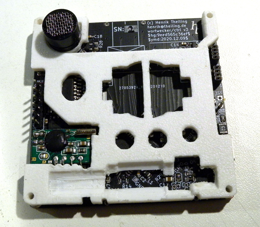
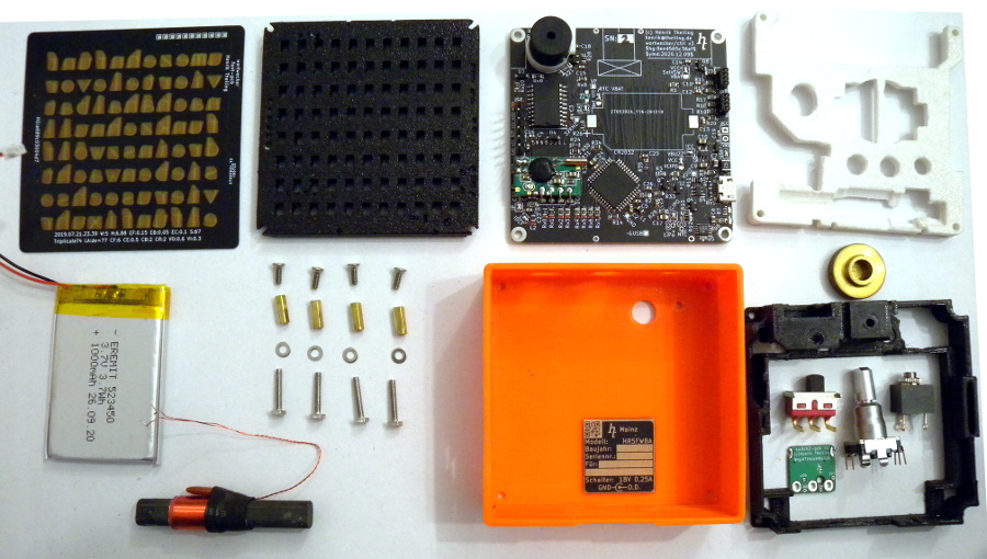 This is an overview of the 'macroscopic' parts, i.e., without the pile of
SMD parts soldered on PCBs.
This is an overview of the 'macroscopic' parts, i.e., without the pile of
SMD parts soldered on PCBs.
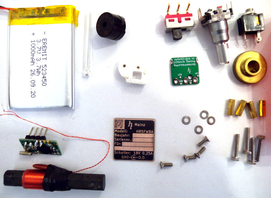 There are more macroscopic parts that are needed: battery, antenna,
ambient light sensor, buzzer, DCF77 module, nuts, bolts, knob,
switches, etc.
There are more macroscopic parts that are needed: battery, antenna,
ambient light sensor, buzzer, DCF77 module, nuts, bolts, knob,
switches, etc.
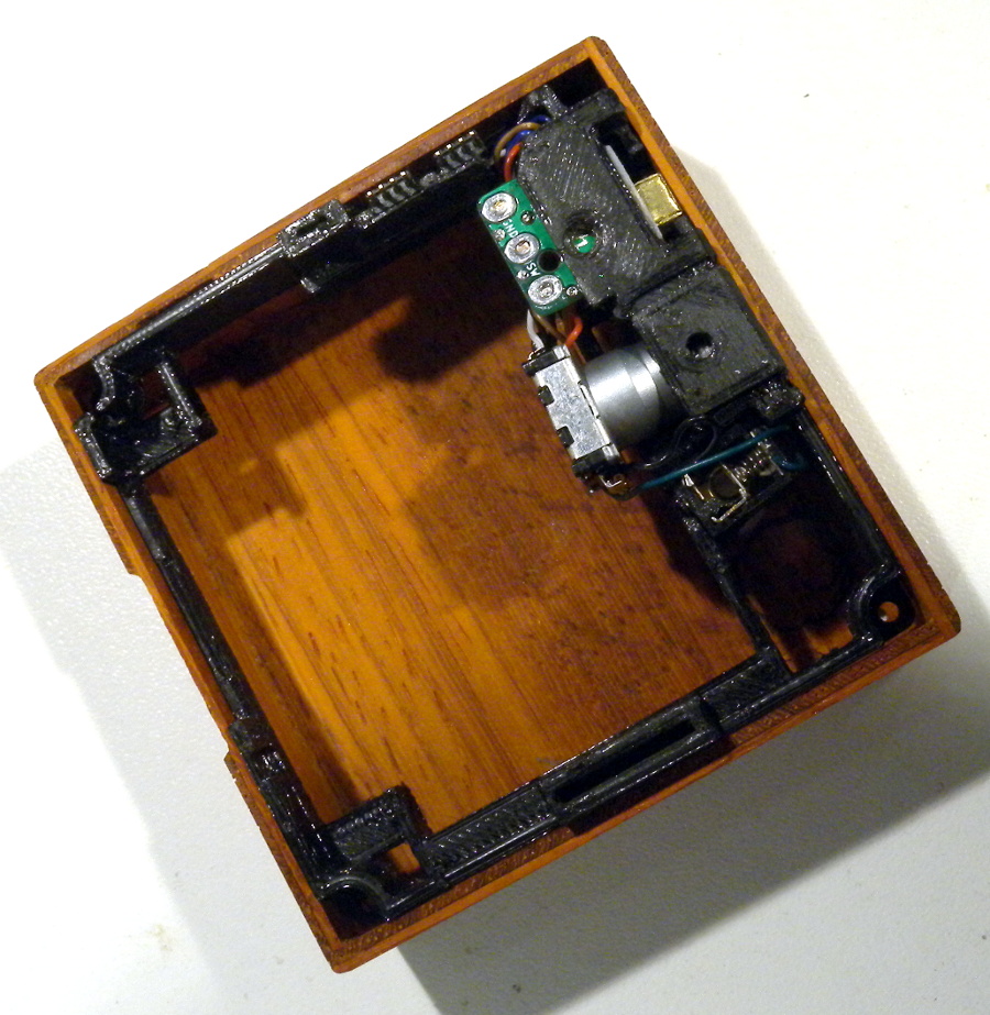 In the prototype clock, the switch module was glued into the enclosure, but
it is separate now. This makes repairs easier, and it was also better when the
enclosure needed cutting and sanding. The switches can be pushed out of their
sockets so that the switch module can be put into the enclosure.
In the prototype clock, the switch module was glued into the enclosure, but
it is separate now. This makes repairs easier, and it was also better when the
enclosure needed cutting and sanding. The switches can be pushed out of their
sockets so that the switch module can be put into the enclosure.
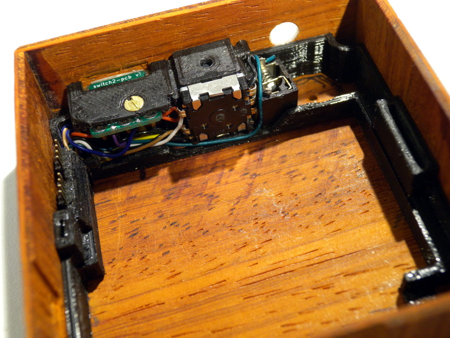 This is the switch module with the switches pushed back into position, and
the alarm on/off switch locked in with a small 2mm bolt. Yeah, I know, it's
not TORX – shame on me.
This is the switch module with the switches pushed back into position, and
the alarm on/off switch locked in with a small 2mm bolt. Yeah, I know, it's
not TORX – shame on me.
 For assembling the clock, the inner parts are stacked together
starting from front to back: the display spacer, the control PCB, and the
mounting frame are bolted together to become the main module sandwich.
After the switch module is inserted into the enclosure, the main module
sandwich can be
inserted to complete the clock.
For assembling the clock, the inner parts are stacked together
starting from front to back: the display spacer, the control PCB, and the
mounting frame are bolted together to become the main module sandwich.
After the switch module is inserted into the enclosure, the main module
sandwich can be
inserted to complete the clock.
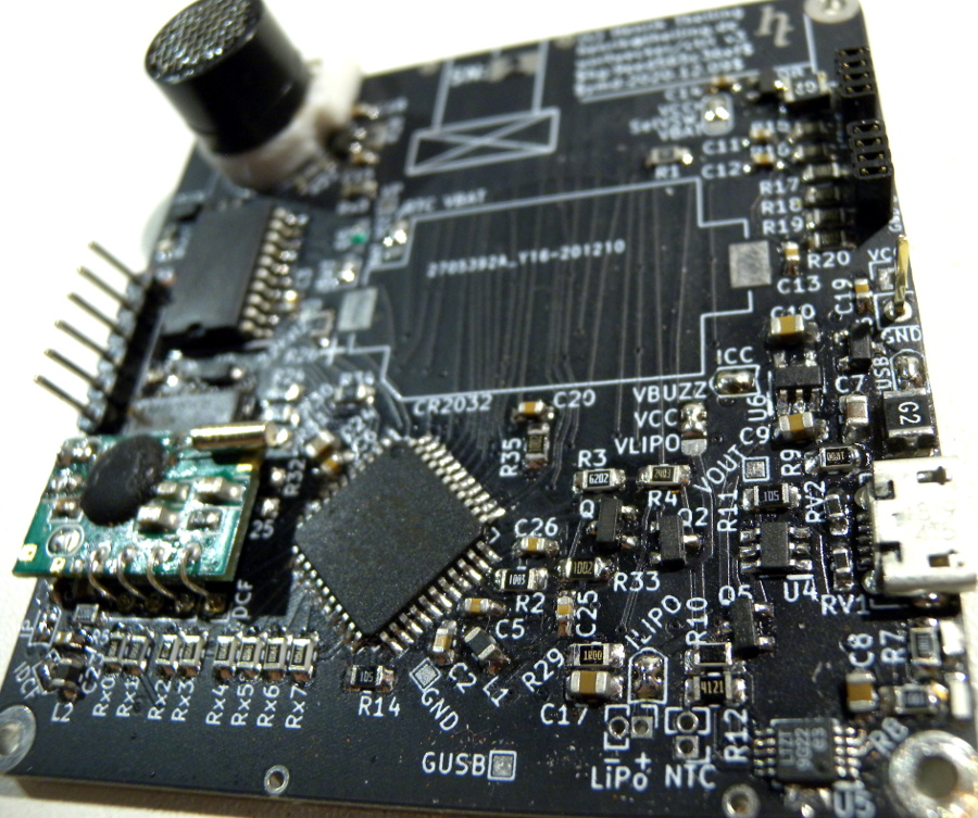 This is the control PCB. It was designed in Kicad just like the
prototype. The evolution of the prototype includes a few improvements,
and I switched from a two-layer to a four-layer PCB, which makes routing
much easier. The CR2032 battery was made optional using a solder switch.
In the end, I did not put in the additional battery, because the lipo
battery can also power the real-time clock without any drawbacks. The clock
needs charging maybe once a year, so a second battery is overkill.
This is the control PCB. It was designed in Kicad just like the
prototype. The evolution of the prototype includes a few improvements,
and I switched from a two-layer to a four-layer PCB, which makes routing
much easier. The CR2032 battery was made optional using a solder switch.
In the end, I did not put in the additional battery, because the lipo
battery can also power the real-time clock without any drawbacks. The clock
needs charging maybe once a year, so a second battery is overkill.
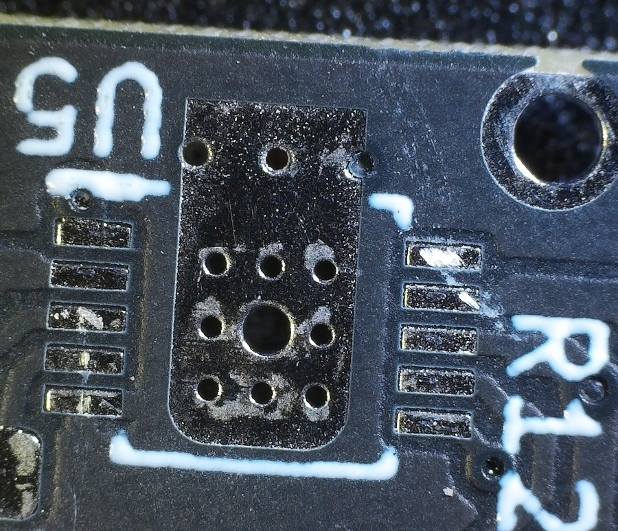
On the left, there's the programming connector, which I might shrink in future projects. It was not in the way in this project, however.
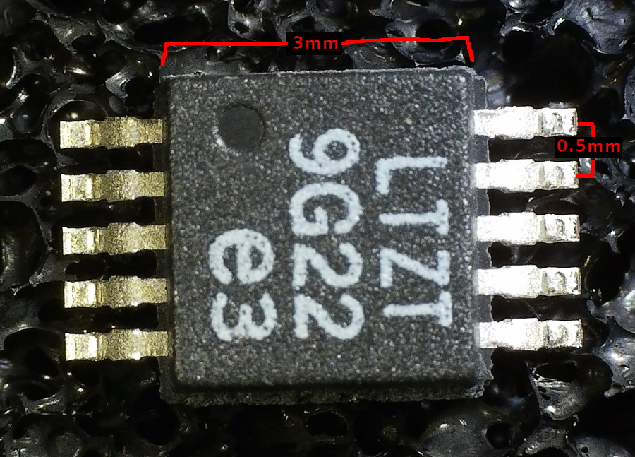 This is the smallest solder job: the lipo charge controller. It is the small chip
on the bottom right in the previous image. I used an LTC4053
in an MSOP-10 package, which is a 3mmx3mm package with 10 pins with a distance of
0.5mm.
This is the smallest solder job: the lipo charge controller. It is the small chip
on the bottom right in the previous image. I used an LTC4053
in an MSOP-10 package, which is a 3mmx3mm package with 10 pins with a distance of
0.5mm.
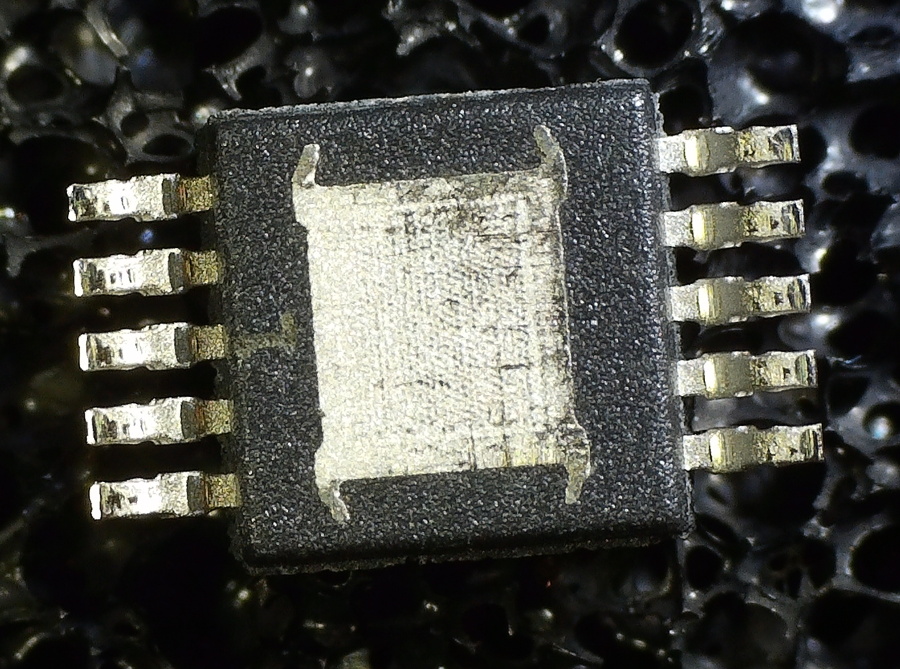 The most difficult problem of soldering this chip is not its mere size, but the
presence of a ground pad on the bottom of the chip that acts as a heat sink. This
needs to be soldered to the PCB, too, preferably to a lot of metal.
The most difficult problem of soldering this chip is not its mere size, but the
presence of a ground pad on the bottom of the chip that acts as a heat sink. This
needs to be soldered to the PCB, too, preferably to a lot of metal.
 To do this soldering manually, I added a pad with several vias so it can be heated
from the back side. Also, the pad extends to the side so heat can be applied from
the side. Luckily, the chip is specified to survive quite a bit of soldering heat.
To do this soldering manually, I added a pad with several vias so it can be heated
from the back side. Also, the pad extends to the side so heat can be applied from
the side. Luckily, the chip is specified to survive quite a bit of soldering heat.
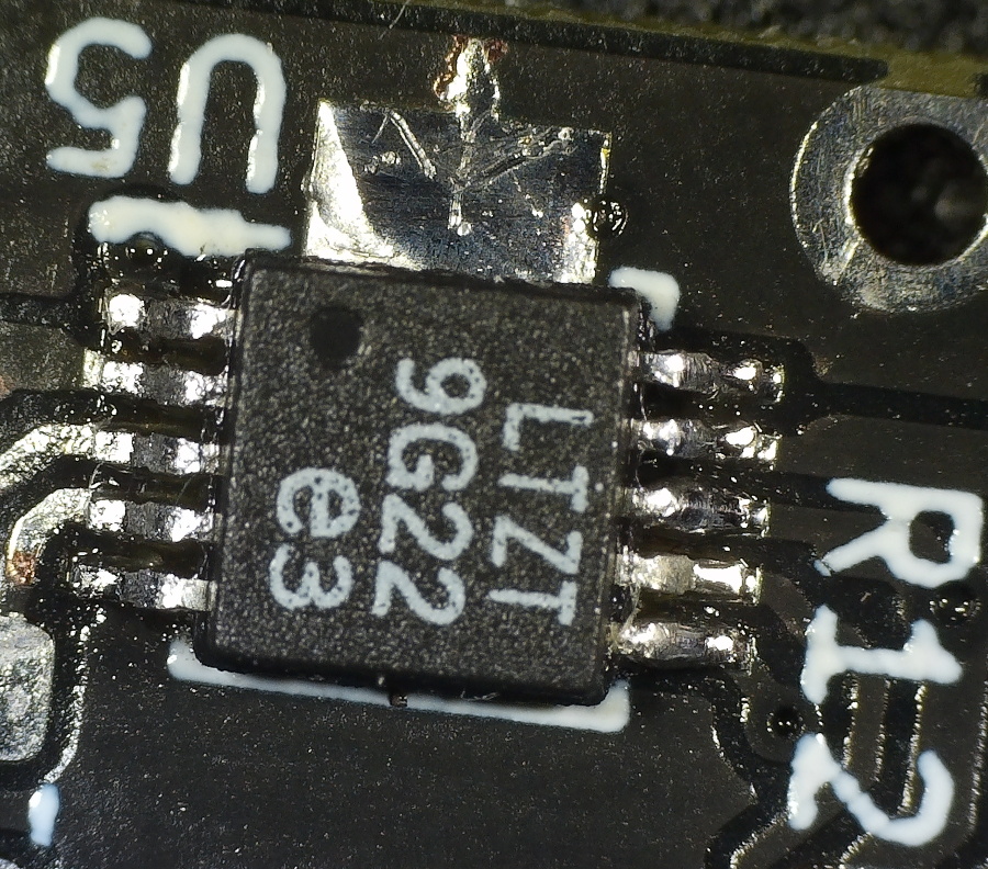 It is totally possible to solder this chip by hand. I did this a few times now and
all chips worked afterwards. The ground pad needs to be attached first, aligning
the chip as accurately as possible. After that, the chip cannot be moved anymore.
It is totally possible to solder this chip by hand. I did this a few times now and
all chips worked afterwards. The ground pad needs to be attached first, aligning
the chip as accurately as possible. After that, the chip cannot be moved anymore.
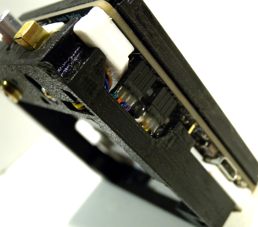
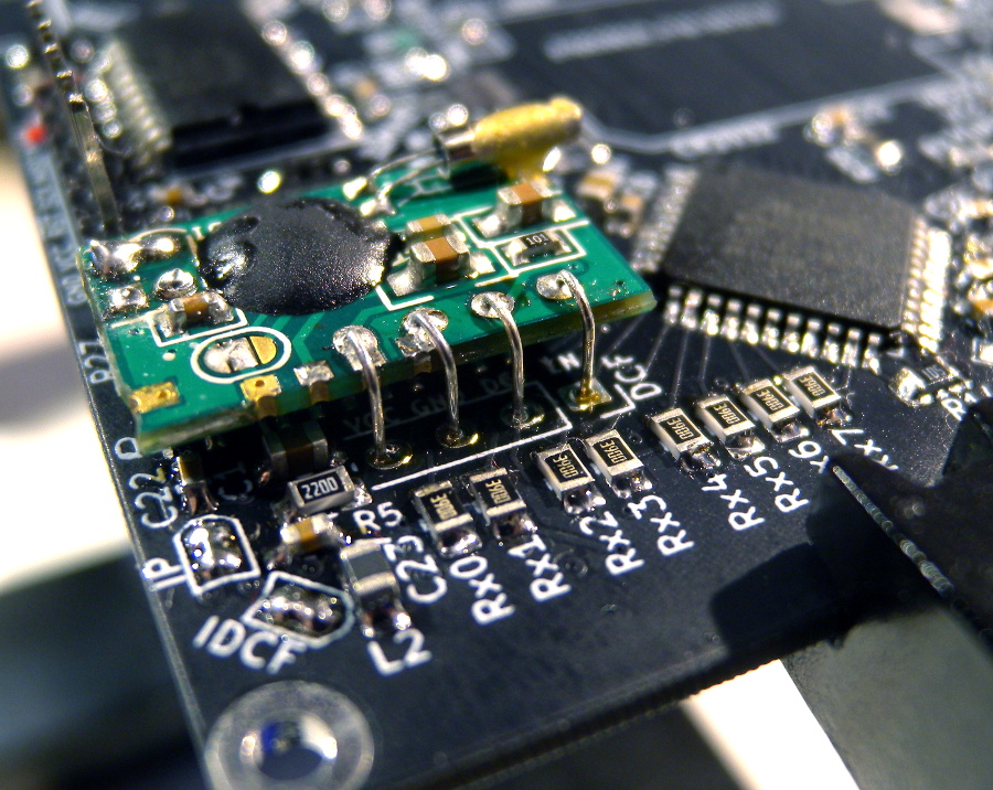 The DCF77 radio clock receiver module is the small piggy-backed PCB below the
programming connector. It is the module from Pollin, which is the smallest I
found. The seemingly weird 3D wire art to attach the module was necessary,
because the module cannot move down without hitting the antenna, and the pin
holes cannot move up, because there are LEDs on the backside of the PCB. I.e.,
there are tight space contraints.
The DCF77 radio clock receiver module is the small piggy-backed PCB below the
programming connector. It is the module from Pollin, which is the smallest I
found. The seemingly weird 3D wire art to attach the module was necessary,
because the module cannot move down without hitting the antenna, and the pin
holes cannot move up, because there are LEDs on the backside of the PCB. I.e.,
there are tight space contraints.
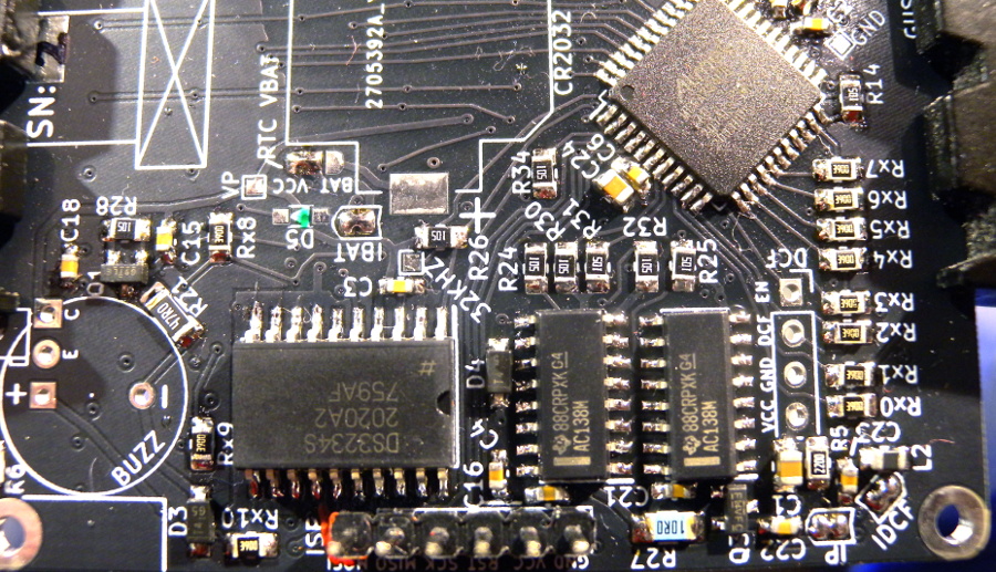 The display driver was changed compared to the prototype where I used a bunch
of transistors. The problem was that the LEDs would flicker faintly from remaining
charges in the wires when switching rows, because the transistors' drains just cut
off the power. The No.2 uses two 74AC138 to get proper push-pull outputs. The
logic family has quite a high output current, just enough to drive a whole row of
low-power LEDs at maximum required brightness.
The display driver was changed compared to the prototype where I used a bunch
of transistors. The problem was that the LEDs would flicker faintly from remaining
charges in the wires when switching rows, because the transistors' drains just cut
off the power. The No.2 uses two 74AC138 to get proper push-pull outputs. The
logic family has quite a high output current, just enough to drive a whole row of
low-power LEDs at maximum required brightness.
The real-time clock is a DS3234, which has an integrated, temperature controlled quartz and uses an SPI bus. I wanted an SPI bus because it draws less power than an I2C bus. It may be overkill, but why not, as this alarm clock is an experiment in low-power applications.
The µ-controller of the clock is an ATMEGA324PB.
 This is the PCB on top of the display spacer and the mounting frame stacked on top.
The mounting frame levels out the electronics so that the lipo and the antenna can
be put on top of this.
This is the PCB on top of the display spacer and the mounting frame stacked on top.
The mounting frame levels out the electronics so that the lipo and the antenna can
be put on top of this.
 The switch PCB can be put on top also outside of the enclosure to complete
the inner part and make a functional alarm clock, only without enclosure.
The switch PCB can be put on top also outside of the enclosure to complete
the inner part and make a functional alarm clock, only without enclosure.
 The switch module attaches to the control module via two small pin headers.
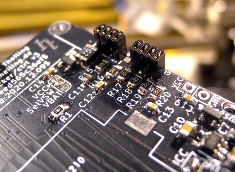 The pin headers are small ones with 1,25mm pin distance.
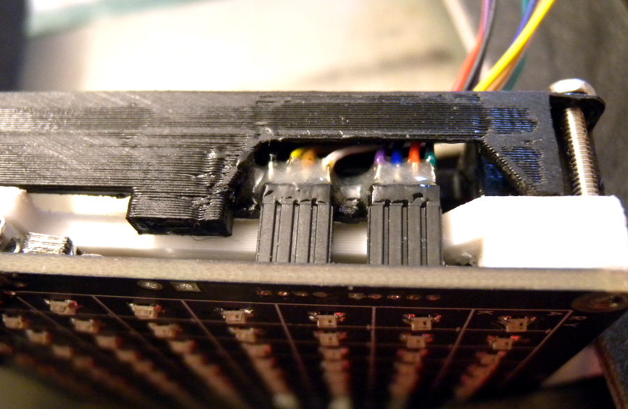 The pins are glued to the switch module. This may seem a bit unelegant, but there
was no space for a proper mechanical connection. The glue has the advantage
that the pin headers can be placed exactly where they belong, after aligning
the sandwiched layers correctly.
The pins are glued to the switch module. This may seem a bit unelegant, but there
was no space for a proper mechanical connection. The glue has the advantage
that the pin headers can be placed exactly where they belong, after aligning
the sandwiched layers correctly.
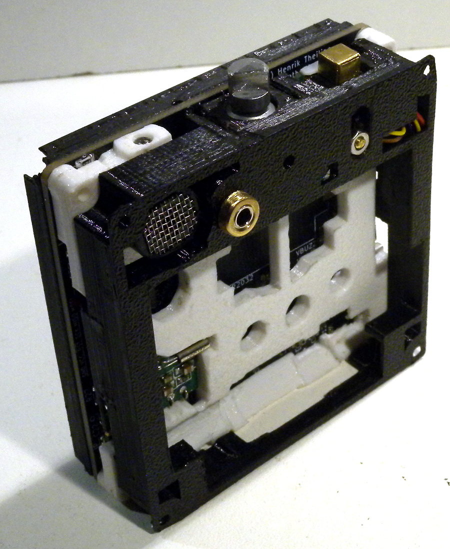 This inner part is a fully functional alarm clock. Also, this sandwich
needs to be quite precisely shaped to insert well into the enclosure, so
in this state, the plastic parts were filed down until they were good.
This inner part is a fully functional alarm clock. Also, this sandwich
needs to be quite precisely shaped to insert well into the enclosure, so
in this state, the plastic parts were filed down until they were good.
In this picture, the lipo and the antenna are not yet attached.
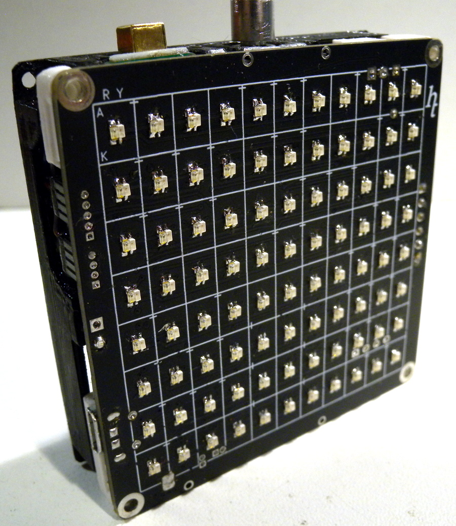 The front without the display spacer shows the PCB's back side with the
176 LEDs.
The front without the display spacer shows the PCB's back side with the
176 LEDs.
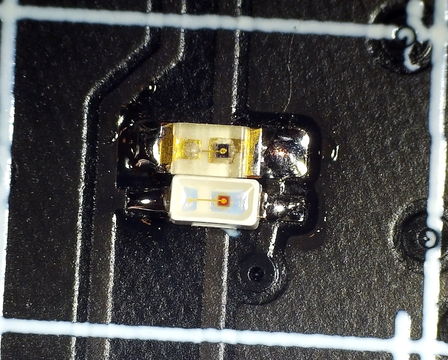 The two leds for each letter are not the same, but were carefully selected for
their colour and also for brightness, a yellow one, and a red one.
The two leds for each letter are not the same, but were carefully selected for
their colour and also for brightness, a yellow one, and a red one.
 I also made a wooden dummy of the inner part with exactly the right
dimensions. This was used to glue up the enclosure, and also to
stabilise the enclosure when handling it, e.g. during sanding.
I also made a wooden dummy of the inner part with exactly the right
dimensions. This was used to glue up the enclosure, and also to
stabilise the enclosure when handling it, e.g. during sanding.
 This is the inner part with the lipo and the antenna attached. These
two parts attach to the mounting frame. The antenna is then soldered
to the PCB. This is the only connection that is not pluggable,
but it simply seemed like overkill to have an antenna connector inside
the clock.
This is the inner part with the lipo and the antenna attached. These
two parts attach to the mounting frame. The antenna is then soldered
to the PCB. This is the only connection that is not pluggable,
but it simply seemed like overkill to have an antenna connector inside
the clock.
 Making the crystal of the clock was a bit of a pain. Sanding glass is not something
I like to do, because the glass dust scares me. I wet sanded by hand at first, which
took forever. When I finally wanted to glue up the face with
the perfectly sized and polished crystal, the gasket of the
vacuum pot failed at almost full vacuum, and the bang knocked
the pot off the table. And, of course, the
crystal inside broke. My ears survived, luckily.
Making the crystal of the clock was a bit of a pain. Sanding glass is not something
I like to do, because the glass dust scares me. I wet sanded by hand at first, which
took forever. When I finally wanted to glue up the face with
the perfectly sized and polished crystal, the gasket of the
vacuum pot failed at almost full vacuum, and the bang knocked
the pot off the table. And, of course, the
crystal inside broke. My ears survived, luckily.
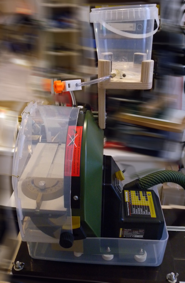 At that point, I got myself a disksander for which I built a water cooling.
Another tool for the workshop. And I got a much better face shield.
Making a new crystal was now much faster and less painful.
At that point, I got myself a disksander for which I built a water cooling.
Another tool for the workshop. And I got a much better face shield.
Making a new crystal was now much faster and less painful.
Oh, and I also had to make a new gasket, which I did from oogoo (starch + silicone clay).
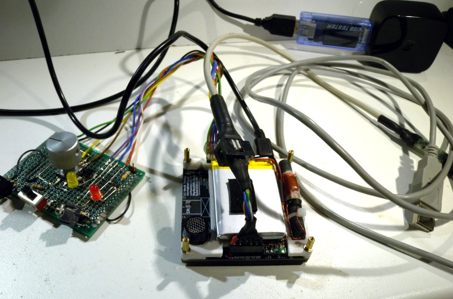 Because I had a working firmware already for the prototype, only little
changes needed to be done, e.g., a new display driver for the 74AC138 chips. While
writing the firmware,
the clock was connected to the programmer, to a USB power supply, and to a mock-up
switch module (on the left) via a special cable.
Because I had a working firmware already for the prototype, only little
changes needed to be done, e.g., a new display driver for the 74AC138 chips. While
writing the firmware,
the clock was connected to the programmer, to a USB power supply, and to a mock-up
switch module (on the left) via a special cable.
This series will be concluded with a third alarm clock soon.